
We have sales items such as analog integrated circuits, MOSFETs, Schottky diodes and passive components, and achieve the most effective management and application in Co-Pak or COB.
We have a MOSFET, analog integrated circuit best design and process integration technical team.
-
Force Mos wafers are mainly self-designed and exclusive technology transferred to cooperative wafer fabs for production. The whole process is supervised and adjusted by the consultant Mr. Xie with years of professional experience, fully controlling the product yield and shortening the production cycle; most competing brands Due to the outsourcing method of wafers, the product quality and production cycle cannot be grasped, and the advantages are lost.
-
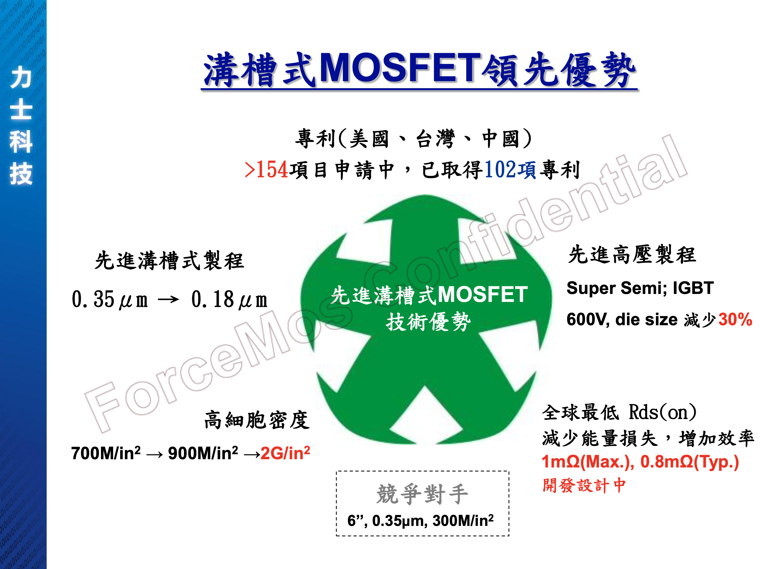
Compared with other competitors, Force Mos uses the most advanced 8" wafers and 0.18μm process in the industry for mass production. Most competitors still use 6" wafers and 0.35/0.25μm process, which has higher cost control. Using the most simplified process technology, the product yield rate can be guaranteed to be greater than 95%.
-
Products with more optimized functions can be developed according to the electrical requirements of the customer's application circuit design.
-
Developed MSD patents and integrated MOSFET, Schottky, and ESD Diode. In addition to leading other manufacturers in technology, it is more in line with customer application requirements.
-
Force Mos has completed the development of the industry’s lowest internal resistance products (RDS(ON)=1.6mΩ(Max.), 1.2mΩ(Typ.)) to improve efficiency and reduce energy consumption.
-
Force Mos has planned to complete the 0.13μm process technology on future product lines.
-
Force Mos has applied for dozens of trench MOSFET and IGBT process and device patents.